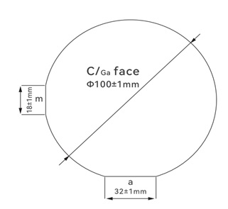
Free-standing GaN Substrates(4″)
| Size (mm) | φ100.0±1.0 | ||||
|---|---|---|---|---|---|
| Thickness (μm) | 420±50 | ||||
| TTV (μm) | ≤30 | ||||
| BOW (μm) | ≤50 | ||||
| RMS (nm) | Ga face:RMS≤0.2 (10μm×10μm); N face:Lapped and etched |
||||
| Orientation | C-plane(0001) off angle toward M-axis 0.3±0.25°; | ||||
| Conduction Type | Un-type | N-type | |||
| (300K) Resistivity (Ω·cm) | ≤0.5 | ≤0.05 | |||
| (300K) Carrier Concentration (cm-3) | ≤2×10¹⁷ | ||||
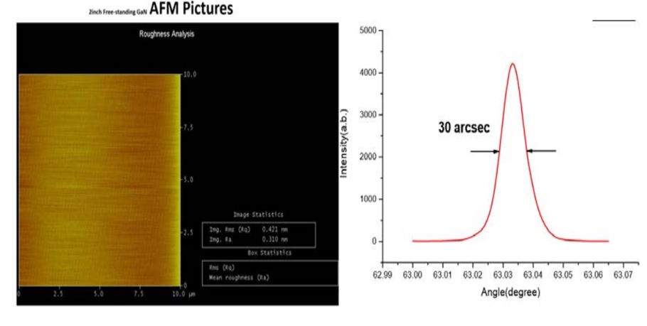
| Dislocation Density (cm-2) | ≤5×10⁶ | ||||
| FWHM(Arcsec) | ~100 | ||||
| Useable Surface Area | >90% | ||||
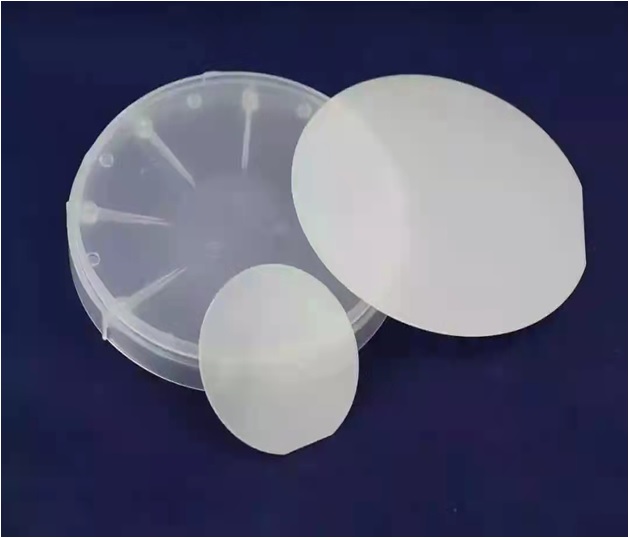
| Package | Packaged in individual containers in a class 100 clean room environment. | ||||
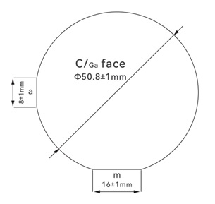
Free-standing GaN Substrates(4″)
| Size (mm) | φ50.8±1.0 | ||||
|---|---|---|---|---|---|
| Thickness (μm) | 400±25 | ||||
| TTV (μm) | ≤15 | ||||
| BOW (μm) | ≤20 | ||||
| RMS (nm) | Ga face:RMS≤0.2 (10μm×10μm); N face:Lapped and etched |
||||
| Orientation | C-plane(0001) off angle toward M-axis 0.3±0.25°; | ||||
| Conduction Type | Un-type | N-Type | SI-Type | ||
| (300K) Resistivity (Ω·cm) | ≤0.5 | ≤0.05 | >106 | ||
| (300K) Carrier Concentration (cm-3) | ≤2×10¹⁷ | ||||
| Dislocation Density (cm-2) | ≤2×10⁶ | ||||
| FWHM(Arcsec) | ~100 | ||||
| Useable Surface Area | >90% | ||||
| Package | Packaged in individual containers in a class 100 clean room environment. | ||||